As the semiconductor industry continues to evolve, wide bandgap (WBG) semiconductors have become essential for next-generation power electronics, RF systems, and high-temperature applications. Materials such as Silicon Carbide (SiC), Gallium Nitride (GaN), Gallium Oxide (Ga₂O₃), and Aluminum Nitride (AlN) are increasingly used because of their superior electrical performance, thermal stability, and efficiency.
A critical process in manufacturing these advanced devices involves the use of gold deplating tools, which are designed to selectively remove gold layers from semiconductor wafers without damaging the underlying structures.
In this article, we explore the role of gold deplating tools, their working mechanisms, benefits, and why they are indispensable in modern wide bandgap semiconductor fabrication.
What Is a Gold Deplating Tool?
A gold deplating tool is a specialized piece of equipment used to remove gold (Au) coatings, contacts, or metallization layers from semiconductor wafers and electronic components. These tools provide precise and controlled removal of gold while protecting sensitive semiconductor materials and surrounding layers.
Gold deplating is commonly used during:
- Device rework and repair
- Process correction
- Metallization adjustments
- Wafer recovery operations
- Selective layer removal during fabrication
Because wide bandgap semiconductor wafers are expensive, manufacturers rely on gold deplating tools to minimize waste and improve production yields.
Why Is Gold Used in Wide Bandgap Semiconductors?
Gold remains one of the most valuable materials in semiconductor manufacturing due to its excellent physical and electrical properties.
Key Advantages of Gold
- Outstanding electrical conductivity
- Excellent corrosion resistance
- High thermal stability
- Strong bonding characteristics
- Reliable performance in harsh environments
Common Applications of Gold Layers
Gold is frequently used in:
- Ohmic contacts
- Bond pads
- Interconnects
- Metal stacks
- RF device structures
- High-power electronic devices
Its reliability makes it ideal for demanding applications such as electric vehicles, renewable energy systems, aerospace electronics, and telecommunications equipment.
Why Is Gold Deplating Necessary?
Although gold is highly beneficial, there are situations where selective removal becomes necessary during manufacturing.
1. Device Rework and Repair
Manufacturing defects can occur during deposition or patterning processes. Instead of discarding an expensive wafer, engineers can remove the gold layer and reprocess the device.
2. Process Corrections
Incorrect metallization patterns or alignment issues may require gold removal before proceeding to the next fabrication stage.
3. Selective Layer Removal
Certain fabrication sequences require temporary gold layers that must later be removed without affecting neighboring structures.
4. Yield Improvement
Gold deplating helps recover partially completed wafers, reducing manufacturing costs and improving overall production efficiency.
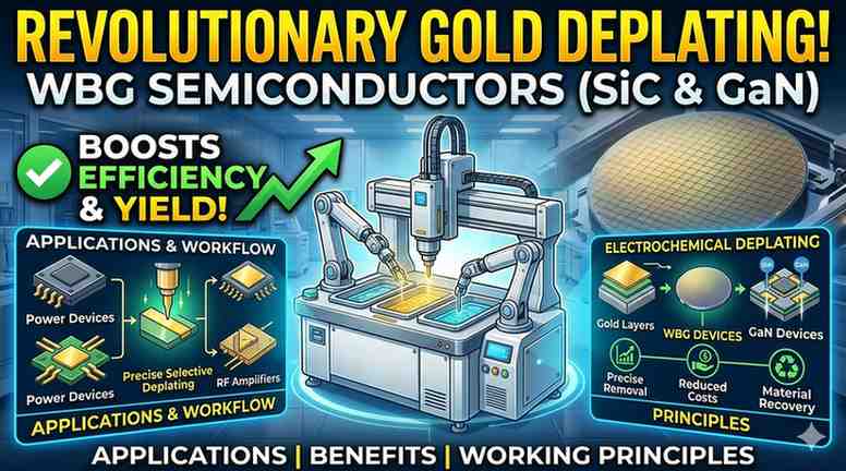
How Does a Gold Deplating Tool Work?
Gold deplating tools are designed to remove gold with high precision while protecting:
- Silicon Carbide (SiC)
- Gallium Nitride (GaN)
- Gallium Oxide (Ga₂O₃)
- Aluminum Nitride (AlN)
- Dielectric layers
- Passivation coatings
- Other metallic structures
Several techniques are commonly used.
Wet Chemical Gold Deplating
Wet chemical etching is one of the most widely used methods.
Common Chemicals
- Potassium Iodide (KI)
- Iodine (I₂)
- Aqua Regia
- Specialized gold etchants
Process Overview
- The wafer is placed in a controlled chemical solution.
- The solution reacts with the gold layer.
- Gold dissolves selectively.
- The wafer is cleaned and inspected.
Advantages
- Cost-effective
- Fast processing
- High removal rates
- Suitable for large-scale production
Electrochemical Gold Deplating
Electrochemical deplating provides a more controlled approach.
How It Works
The wafer acts as an electrode within an electrolytic system. By applying a controlled electrical current, gold is selectively dissolved and removed.
Benefits
- Exceptional precision
- Reduced chemical consumption
- Better selectivity
- Minimal substrate damage
- Improved process control
This technique is often preferred for high-value semiconductor devices.
Plasma-Based Gold Removal
Although less common, plasma-assisted methods may be used in specialized applications.
Features
- Dry processing
- Reduced liquid chemical usage
- High cleanliness
- Precise material removal
However, due to gold’s chemical properties, plasma-based removal is generally more complex and less widely adopted than wet or electrochemical methods.
Requirements for Gold Deplating in Wide Bandgap Manufacturing
Wide bandgap semiconductor wafers are expensive and highly sensitive. Therefore, gold deplating systems must meet strict performance requirements.
High Selectivity
The tool must remove gold without attacking:
- Semiconductor materials
- Dielectric films
- Underlying metallization
Precision Control
Modern semiconductor devices contain microscopic structures that require accurate and repeatable processing.
Low Contamination Risk
Contamination can significantly reduce device performance and reliability.
Minimal Substrate Damage
The process must preserve:
- Surface integrity
- Electrical characteristics
- Thermal performance
Cleanroom Compatibility
Gold deplating equipment must operate within semiconductor cleanroom environments to maintain manufacturing standards.
Applications of Gold Deplating Tools
Gold deplating systems are widely used across various semiconductor sectors.
Power Electronics
Used in:
- Electric vehicle inverters
- Industrial motor drives
- Power conversion systems
RF and Microwave Devices
Essential for:
- 5G communication equipment
- Radar systems
- Satellite communication devices
Aerospace and Defense
Supports fabrication of:
- High-reliability electronics
- Advanced sensing systems
- Military communication hardware
Renewable Energy Systems
Used in semiconductor devices powering:
- Solar energy systems
- Wind energy converters
- Smart grid infrastructure
Benefits of Using Gold Deplating Tools
Manufacturers gain several advantages by incorporating advanced gold deplating solutions.
Reduced Manufacturing Costs
Recovering wafers reduces material waste and lowers production expenses.
Improved Production Yield
Defective metallization layers can be corrected rather than discarded.
Enhanced Process Flexibility
Engineers can make adjustments during fabrication without restarting the entire process.
Better Quality Control
Selective removal enables more accurate process optimization and inspection.
Increased Sustainability
Reducing wafer scrap supports environmentally responsible manufacturing practices.
Future of Gold Deplating Technology
As wide bandgap semiconductor adoption continues to grow, gold deplating technologies are expected to become even more advanced.
Future developments may include:
- AI-assisted process monitoring
- Automated wafer handling systems
- Environmentally friendly etchants
- Enhanced electrochemical control
- Greater integration with smart semiconductor fabs
These innovations will help manufacturers achieve higher yields, lower costs, and improved device performance.
Frequently Asked Questions (FAQ)
What is a gold deplating tool?
A gold deplating tool is specialized equipment used to selectively remove gold layers from semiconductor wafers and electronic devices during manufacturing, repair, or rework processes.
Why is gold used in wide bandgap semiconductors?
Gold provides excellent conductivity, corrosion resistance, thermal stability, and reliability, making it ideal for contacts, interconnects, and bonding applications.
Which wide bandgap materials use gold metallization?
Common materials include Silicon Carbide (SiC), Gallium Nitride (GaN), Gallium Oxide (Ga₂O₃), and Aluminum Nitride (AlN).
What are the main gold removal methods?
The most common methods include wet chemical etching, electrochemical deplating, and specialized plasma-based techniques.
Why is selective gold removal important?
Selective removal prevents damage to expensive semiconductor wafers and allows manufacturers to correct process errors without scrapping the entire device.
Conclusion
Gold deplating tools play a vital role in wide bandgap semiconductor manufacturing, enabling precise and selective removal of gold layers while protecting valuable semiconductor materials. As demand for high-performance power electronics, RF devices, and advanced communication systems continues to rise, these tools will remain essential for improving manufacturing efficiency, reducing costs, and ensuring reliable device performance.
Their ability to support rework, repair, and process optimization makes gold deplating technology a key component of modern semiconductor fabrication workflows.